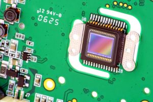
When it comes to the relative advantages of CMOS versus CCD images, it seems that the debate has continued for as long as most people can remember. Since there is no definitive conclusion in sight, it’s not surprising that the answer is elusive, as the topic isn’t static. Not only is technology advancing, but markets continue to evolve. This affects what is technically feasible, but also what is commercially viable. Imaging applications are varied, with different and changing requirements. Some applications are best served by CMOS imagers, some by CCD’s.
 CCD (charge coupled devise) and CMOS (Complementary Metal Oxide Semiconductor) image sensors are two different technologies that are used to capture images digitally. Each has unique strengths and weaknesses giving advantages in different applications.
Both imagers were invented in the late 1960’s and 70’s. Because of the ability to provide a superior image in relationship to fabrication technology, CCD became dominant. CMOS image sensors required more uniformity and smaller features than silicon wafer foundries could deliver at the time. It wasn’t until the 1990’s that lithography developed to the point that designers could begin making a case for using CMOS imagers again. The renewed interest was based on expectations of lowered power consumption, camera-on-a-chip integration, and lowered fabrication costs from the reuse of mainstream logic and memory device fabrication. Achieving these benefits while delivering high-image quality has taken more time and process adaptation than the original projections suggested, but, CMOS imagers have joined CCDs as mainstream, mature technology.
The advent of CCD marked the end of vacuum tube imagers used in televisions as it overcame the disadvantages like chronic picture artifacts as lag and burn-in, fragility of large glass tubes or the sensitivity to shock. It also marked the beginning of a new era in imaging systems. For quite a number of years, it enjoyed quality advantages over the rival CMOS sensors. Wherever quality was paramount, CCDs were preferred. CMOS was used mainly in applications where small size and low power was the motivating requirements.
Both CCD and CMOS image sensors use large arrays of thousands (sometimes millions) of photo-sites, commonly called pixels. Both carry out same steps.
Light-to-charge conversion
Incident light is directed by the micro-lens (a tiny lens placed over the pixel to increase its effective size and thereby fill factor) onto the photo-sensitive area of each pixel where it is converted into electrons that collect in a semiconductor “bucket.”
The bigger the pixel, the greater amount of light it can collect. Thus, big pixel sensors work best under low-light conditions. For the same number of pixels, bigger pixels results in bigger chip, this means higher cost. Conversely, smaller pixels enable smaller chip sizes and lower chip prices, as well as lower lens costs. But there are limitations on pixel size reduction. Smaller pixels are less sensitive to light, the optics required to resolve the pixels becomes expensive and requires expensive fabrication possesses.
Charge accumulation
As more light enters, more electrons accumulate into the bucket.
Transfer
Accumulated charge must be transferred to the signal conditioning and processing circuitry.
Charge-to-voltage conversion
The accumulated charge must be output as the voltage signal.
Amplification
Voltage signal is then amplified before it is fed to the camera circuitry.
Both perform the above tasks. The aspect in which they differ is the order of execution of these tasks.
For example, CMOS imagers are preferred over CCDs for machine vision. For machine vision, the key parameters are speed and noise. High speed CMOS imagers can be designed to have much lower noise versus high speed CCDs.
Conversely, CCDs are a better choice when it comes to near infrared imaging. Most CMOS imager fabrication processes are tuned for high volume applications that only image in the visible, and are not very sensitive to the near infrared. CCDs that are specifically designed to be highly sensitive in the near infrared are much more sensitive than CMOS imagers.
With these complexities at play, it is not surprising that it is impossible to make a general statement about CMOS versus CCD imagers that applies to all applications. Perhaps the debate can be settled based on the specific application of use. At Universe Optics, we manufacture precision lenses for use in multiple disciplines. Our designs are used in machine vision, near infrared technology, Lidar technology and many other areas. We work with your specifications to deliver lenses designed to give clarity to any application.