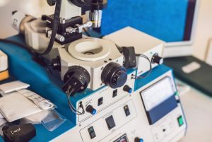
TEM, or Transmission electron microscopy (also sometimes conventional transmission electron microscopy or CTEM) is a microscopy technique in which a beam of electrons is transmitted through a specimen to form an image. The specimen is most often an ultrathin section less than 100 nm thick or a suspension on a grid. An image is formed from the interaction of the electrons with the sample as the beam is transmitted through the specimen. The image is then magnified and focused onto an imaging device, such as a fluorescent screen, a layer of photographic film, or a sensor such as a charge-coupled device.
 A transmission electron microscopes is capable of imaging at a significantly higher resolution than light microscopes, owing to the smaller de Broglie wavelength of electrons. This enables the instrument to capture fine detail—even as small as a single column of atoms, which is thousands of times smaller than a resolvable object seen in a light microscope. Transmission electron microscopy is a major analytical method in the physical, chemical and biological sciences. TEMs find application in cancer research, virology, and materials science as well as pollution, nanotechnology and semiconductor research.
At lower magnifications, TEM image contrast is due to differential absorption of electrons by the material due to differences in composition or thickness of the material. At higher magnifications, complex wave interactions modulate the intensity of the image, requiring expert analysis of observed images. Alternate modes of use allow for the TEM to observe modulations in chemical identity, crystal orientation, electronic structure and sample induced electron phase shift as well as the regular absorption-based imaging.
The highest-magnification image ever was recently obtained using a transmission electron microscope. The image reveals the atoms in a two-dimensional self-supporting sheet of a semiconductor, and has a resolution of 0.39 ångströms; for comparison, most atoms are about 2–4 Å in diameter. The technique might eventually allow 2D materials to be examined with unprecedented precision, providing insight into this burgeoning class of useful compounds. It might also lead to the development of a method that can image individual atoms in 3D objects.
Transmission electron microscope (TEM), is a type of electron microscope that has three essential systems:
- an electron gun, which produces the electron beam, and the condenser system, which focuses the beam onto the object
- the image-producing system, consisting of the objective lens, movable specimen stage, and intermediate and projector lenses, which focus the electrons passing through the specimen to form a real, highly magnified image
- the image-recording system, which converts the electron image into some form perceptible to the human eye. The image-recording system usually consists of a fluorescent screen for viewing and focusing the image and a digital camera for permanent records. In addition, a vacuum system, consisting of pumps and their associated gauges and valves, and power supplies are required.
To generate the image, a method called ptychography in which radiation — in this case, electrons — is passed through a specimen to produce many 2D diffraction patterns. The basic principle of the technique was proposed almost 50 years ago by the physicist Walter Hoppe, who reasoned that there should be enough information in the diffraction data to work backwards to produce an image of the diffracting object. However, it was many years before computer algorithms were developed that could do this reverse calculation easily and reliably. The pictures produced by ptychographic methods are generated using a computer from a vast amount of indirect scattering data.
Perhaps the take-home message of this work is not so much the record resolution, or its applications to 2D materials, but the fact that it will provide a way of precisely imaging the 3D bonding of every individual atom in a solid volume of matter, while using a minimal flux of damaging electrons.
Universe Kogaku designs and manufactures optical lenses for medical imaging, security, high tech and electronic applications. We stock 1000’s of standard lens assemblies and can custom design a solution for scanners, CCTV, CCD/CMOS, medical imaging, surveillance systems, machine vision and night vision systems.